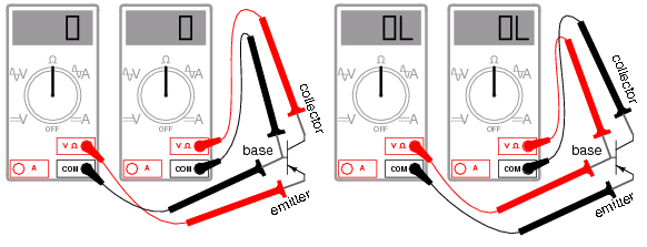
Bipolar transistors are constructed of a three-layer semiconductor “sandwich,” either PNP or NPN. As such, transistors register as two diodes connected back-to-back when tested with a multimeter's “resistance” or “diode check” function as illustrated in Figure below. Low resistance readings on the base with the black negative (-) leads correspond to an N-type base in a PNP transistor. On the symbol, the N-type material corresponds to the “non-pointing” end of the base-emitter junction, the base. The P-type emitter corresponds to “pointing” end of the base-emitter junction the emitter.

PNP transistor meter check: (a) forward B-E, B-C, resistance is low; (b) reverse B-E, B-C, resistance is ∞.
Here I'm assuming the use of a multimeter with only a single continuity range (resistance) function to check the PN junctions. Some multimeters are equipped with two separate continuity check functions: resistance and “diode check,” each with its own purpose. If your meter has a designated “diode check” function, use that rather than the “resistance” range, and the meter will display the actual forward voltage of the PN junction and not just whether or not it conducts current.
Meter readings will be exactly opposite, of course, for an NPN transistor, with both PN junctions facing the other way. Low resistance readings with the red (+) lead on the base is the “opposite” condition for the NPN transistor.
If a multimeter with a “diode check” function is used in this test, it will be found that the emitter-base junction possesses a slightly greater forward voltage drop than the collector-base junction. This forward voltage difference is due to the disparity in doping concentration between the emitter and collector regions of the transistor: the emitter is a much more heavily doped piece of semiconductor material than the collector, causing its junction with the base to produce a higher forward voltage drop.
Knowing this, it becomes possible to determine which wire is which on an unmarked transistor. This is important because transistor packaging, unfortunately, is not standardized. All bipolar transistors have three wires, of course, but the positions of the three wires on the actual physical package are not arranged in any universal, standardized order.
Suppose a technician finds a bipolar transistor and proceeds to measure continuity with a multimeter set in the “diode check” mode. Measuring between pairs of wires and recording the values displayed by the meter, the technician obtains the data in Figure below.
 |
|
Unknown bipolar transistor. Which terminals are emitter, base, and collector? Ω-meter readings between terminals.
The only combinations of test points giving conducting meter readings are wires 1 and 3 (red test lead on 1 and black test lead on 3), and wires 2 and 3 (red test lead on 2 and black test lead on 3). These two readings must indicate forward biasing of the emitter-to-base junction (0.655 volts) and the collector-to-base junction (0.621 volts).
Now we look for the one wire common to both sets of conductive readings. It must be the base connection of the transistor, because the base is the only layer of the three-layer device common to both sets of PN junctions (emitter-base and collector-base). In this example, that wire is number 3, being common to both the 1-3 and the 2-3 test point combinations. In both those sets of meter readings, the black (-) meter test lead was touching wire 3, which tells us that the base of this transistor is made of N-type semiconductor material (black = negative). Thus, the transistor is a PNP with base on wire 3, emitter on wire 1 and collector on wire 2 as described in Figure below.
 |
|
BJT terminals identified by Ω-meter.
Please note that the base wire in this example is not the middle lead of the transistor, as one might expect from the three-layer “sandwich” model of a bipolar transistor. This is quite often the case, and tends to confuse new students of electronics. The only way to be sure which lead is which is by a meter check, or by referencing the manufacturer's “data sheet” documentation on that particular part number of transistor.
Knowing that a bipolar transistor behaves as two back-to-back diodes when tested with a conductivity meter is helpful for identifying an unknown transistor purely by meter readings. It is also helpful for a quick functional check of the transistor. If the technician were to measure continuity in any more than two or any less than two of the six test lead combinations, he or she would immediately know that the transistor was defective (or else that it wasn't a bipolar transistor but rather something else -- a distinct possibility if no part numbers can be referenced for sure identification!). However, the “two diode” model of the transistor fails to explain how or why it acts as an amplifying device.
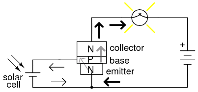
To better illustrate this paradox, let's examine one of the transistor switch circuits using the physical diagram in Figure below rather than the schematic symbol to represent the transistor. This way the two PN junctions will be easier to see.

A small base current flowing in the forward biased base-emitter junction allows a large current flow through the reverse biased base-collector junction.
A grey-colored diagonal arrow shows the direction of electron flow through the emitter-base junction. This part makes sense, since the electrons are flowing from the N-type emitter to the P-type base: the junction is obviously forward-biased. However, the base-collector junction is another matter entirely. Notice how the grey-colored thick arrow is pointing in the direction of electron flow (up-wards) from base to collector. With the base made of P-type material and the collector of N-type material, this direction of electron flow is clearly backwards to the direction normally associated with a PN junction! A normal PN junction wouldn't permit this “backward” direction of flow, at least not without offering significant opposition. However, a saturated transistor shows very little opposition to electrons, all the way from emitter to collector, as evidenced by the lamp's illumination!
Clearly then, something is going on here that defies the simple “two-diode” explanatory model of the bipolar transistor. When I was first learning about transistor operation, I tried to construct my own transistor from two back-to-back diodes, as in Figure below.

A pair of back-to-back diodes don't act like a transistor!
My circuit didn't work, and I was mystified. However useful the “two diode” description of a transistor might be for testing purposes, it doesn't explain how a transistor behaves as a controlled switch.
What happens in a transistor is this: the reverse bias of the base-collector junction prevents collector current when the transistor is in cutoff mode (that is, when there is no base current). If the base-emitter junction is forward biased by the controlling signal, the normally-blocking action of the base-collector junction is overridden and current is permitted through the collector, despite the fact that electrons are going the “wrong way” through that PN junction. This action is dependent on the quantum physics of semiconductor junctions, and can only take place when the two junctions are properly spaced and the doping concentrations of the three layers are properly proportioned. Two diodes wired in series fail to meet these criteria; the top diode can never “turn on” when it is reversed biased, no matter how much current goes through the bottom diode in the base wire loop. See Bipolar junction transistors, Ch 2 for more details.
That doping concentrations play a crucial part in the special abilities of the transistor is further evidenced by the fact that collector and emitter are not interchangeable. If the transistor is merely viewed as two back-to-back PN junctions, or merely as a plain N-P-N or P-N-P sandwich of materials, it may seem as though either end of the transistor could serve as collector or emitter. This, however, is not true. If connected “backwards” in a circuit, a base-collector current will fail to control current between collector and emitter. Despite the fact that both the emitter and collector layers of a bipolar transistor are of the same doping type (either N or P), collector and emitter are definitely not identical!
Current through the emitter-base junction allows current through the reverse-biased base-collector junction. The action of base current can be thought of as “opening a gate” for current through the collector. More specifically, any given amount of emitter-to-base current permits a limited amount of base-to-collector current. For every electron that passes through the emitter-base junction and on through the base wire, a certain, number of electrons pass through the base-collector junction and no more.
In the next section, this current-limiting of the transistor will be investigated in more detail.
REVIEW:
Tested with a multimeter in the “resistance” or “diode check” modes, a transistor behaves like two back-to-back PN (diode) junctions.
The emitter-base PN junction has a slightly greater forward voltage drop than the collector-base PN junction, because of heavier doping of the emitter semiconductor layer.
The reverse-biased base-collector junction normally blocks any current from going through the transistor between emitter and collector. However, that junction begins to conduct if current is drawn through the base wire. Base current may be thought of as “opening a gate” for a certain, limited amount of current through the collector.
No comments:
Post a Comment